RS4T245XTSS16

RS4T245 4-Bit Dual-Supply Bus Transceiver with Configurable Voltage Translation and 3-State Output FEATURES • • • • • Control Inputs VIH/VIL Levels are Referenced to VCCA Voltage Power-Supply Range: VCCA and VCCB:1.65V to 5.5V VCC Isolation: If Either VCC is at GND, Both Ports are in the High-Impedance State IOFF: Supports Partial-Power-Down Mode Operation Extended Temperature: -40°C to +125°...
развернуть ▼ свернуть ▲
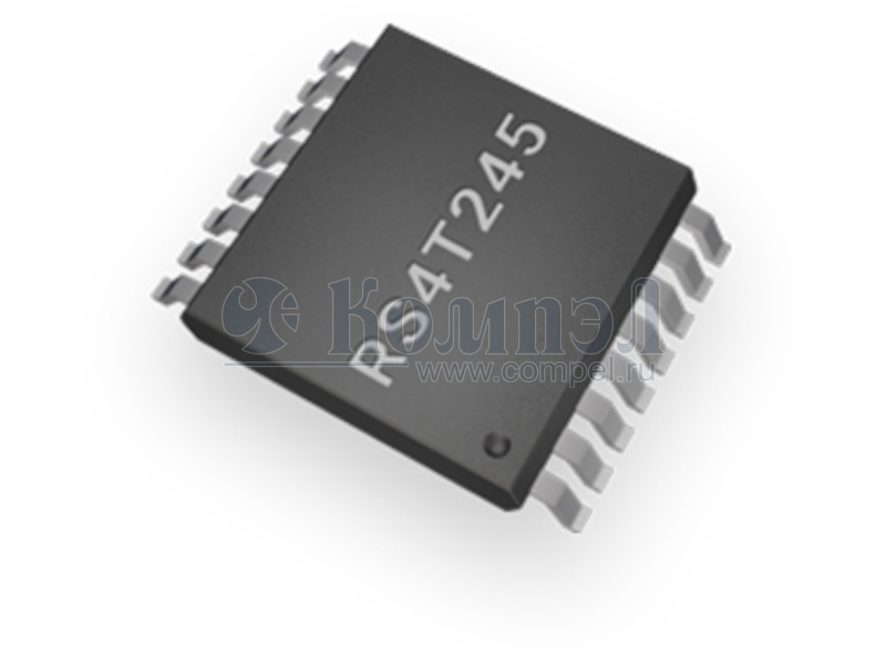
Технические характеристики

показать свернуть
Корпус TSSOP-16
Тип выходного сигнала
Особенности
Напряжение питания входа
Напряжение питания выхода
Нашли ошибку? Выделите её курсором и нажмите CTRL + ENTER

Файлы 1

показать свернуть
RS4T245 4-Bit Dual-Supply Bus Transceiver with Configurable Voltage Translation and 3-State Output FEATURES • • • • • Control Inputs VIH/VIL Levels are Referenced to VCCA Voltage Power-Supply Range: VCCA and VCCB:1.65V to 5.5V VCC Isolation: If Either VCC is at GND, Both Ports are in the High-Impedance State IOFF: Supports Partial-Power-Down Mode Operation Extended Temperature: -40°C to +125°C APPLICATIONS • • • • Desktop PC Personal electronics Industrial Enterprise DESCRIPTION This 4-bit non-inverting bus transceiver is a bidirectional voltage-level translator and can be used to establish digital switching compatibility between mixed-voltage systems. It uses two separate configurable power-supply rails, Both VCCA and VCCB supporting operating voltages from 1.65 V to 5.5 V, A ports, DIR and ̅̅̅̅ OE tracks the VCCA supply and B ports tracks the VCCB supply. This allows the support of both lower and higher logic signal levels while providing bidirectional translation capabilities between any of the 1.8V, 2.5V, 3.3V and 5.5V voltage nodes. The RS4T245 is designed for asynchronous communication between two data buses. The logic levels of the ̅̅̅̅ ) direction-control (DIR) input and the output-enable ( OE input activate either the B-port outputs or the A-port outputs or place both output ports into the high-impedance mode. The device transmits data from the A bus to the B bus when the B-port outputs are activated, and from the B bus to the A bus when the A-port outputs are activated. The input circuitry on both A and B ports is always active and must have a logic HIGH or LOW level applied to prevent excess ICC and ICCZ. This device is fully specified for partial-power-down applications using IOFF. The IOFF circuitry disables the outputs, preventing damaging current backflow through the device when it is powered down. The VCC isolation feature ensures that if either VCC input is at GND, all outputs are in the high-impedance state. To ensure the high-impedance state during power up or power down, ̅̅̅̅ OE should be tied to VCC through a pullup resistor, the minimum value of the resistor is determined by the current-sinking capability of the driver. The RS4T245 is designed so that the control pins (DIR and ̅̅̅̅ ) are supplied by VCCA. It operates over an ambient OE temperature range of -40°C to +125°C. Device Information (1) (1) REV A.1 PART NUMBER PACKAGE BODY SIZE (NOM) TSSOP16(16) 5.00mm×4.40mm RS4T245 QFN2.6x1.8-16L 2.60mm×1.80mm QFN2.5x3.5-16L 2.50mm×3.50mm For all available packages, see the orderable addendum at the end of the data sheet. 1 / 17 www.run-ic.com PDF
Документация на серию RS4T245 

Дата модификации: 07.04.2022

Размер: 603.1 Кб

17 стр.

    Внимание! Точность указанного на сайте описания товара не может быть гарантирована. Для получения более полной и точной информации о товаре смотрите техническое описание (Datasheet) на сайте производителя.