
13 октября 2022
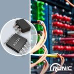
новость
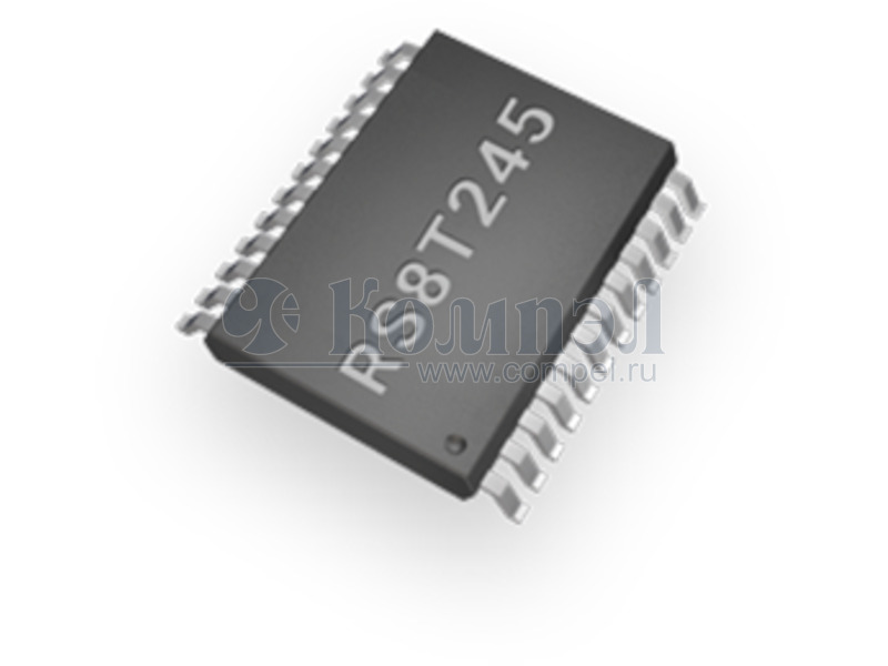
| Корпус | TSSOP-24 | |
|---|---|---|
| Тип выходного сигнала |  | |
| Особенности |  | |
| Напряжение питания входа |  | |
| Напряжение питания выхода |  |
Внимание! Точность указанного на сайте описания товара не может быть гарантирована. Для получения более полной и точной информации о товаре смотрите техническое описание (Datasheet) на сайте производителя.